


Abstract
Inkjet printing technique provides a low-cost way for large-area construction of the patterned organic semiconductors toward integrated organic electronics. However, because of a lack of control over the wetting and dewetting dynamics of organic inks, inkjet-printed organic semiconductor crystals (OSCCs) are frequently plagued by the 'coffee ring' effect and uncontrollable growth process, leading to an uneven crystal morphology and disordered orientation. Here, we report a universal microchannel-assisted inkjet printing (MA-IJP) method for patterning of OSCC arrays with ordered crystallographic orientation. The micro-sized channel template not only provides a unidirectional capillary force to guide the wetting process of organic inks, but also confines the evaporation-induced dewetting behavior, enabling the long-range ordered growth of OSCCs. The patterned 2,7-dioctyl[1]benzothieno[3,2-b][1]benzothiophene (C8-BTBT) crystals present one-dimensional structures with a pure (010) crystallographic orientation. The 7 × 7 discrete organic field-effect transistor array made from the patterned C8-BTBT crystals exhibits a high average mobility up to 3.23 cm2 V−1 s−1 with a maximum mobility of 5.36 cm2 V−1 s−1. Given the good generality of the patterning process and high quality of the obtained OSCC crystal array, it is anticipated that our MA-IJP approach will constitute a major step toward integrated electronic and optoelectronic devices.
Export citation and abstract BibTeX RIS

Original content from this work may be used under the terms of the Creative Commons Attribution 4.0 license. Any further distribution of this work must maintain attribution to the author(s) and the title of the work, journal citation and DOI.
1. Introduction
Precise patterning of well-oriented organic semiconductor crystal (OSCC) arrays with a uniform structure is of great significance in the efficient integration of high-performance circuits based on organic field-effect transistors (OFETs) [1–5]. In the last decade, various techniques, such as surface-selective deposition [6, 7], inkjet printing [1, 8, 9], and transfer printing [10], have been developed for the simultaneous patterning and alignment of OSCCs. Among them, inkjet printing provides a considerable potential to control the deposition position of organic semiconductors for realizing patterned OSCCs. Unfortunately, the printed OSCCs suffer from uneven pattern architectures, stochastic orientation, as well as disordered molecular packing, which will inevitably cause performance degeneration of OFETs and restrict their practical applications [11–13]. Therefore, the core challenges are focused on inkjet printing of the OSCCs synchronized with regulation of structure and crystallographic orientation.
In a typical inkjet-printing process, ink droplets are ejected onto the specified locations of a substrate surface, followed by wetting and dewetting processes [14–17]. The solution wetting behavior determines the deposition position of organic crystals and the uncontrolled wetting will result in the reduction of the intended resolution of the yielded OSCC patterns [18]. The dewetting process is driven by the droplet evaporation and thus plays a crucial role in the crystallization order and the architectures of the organic crystals [1, 19]. During the traditional inkjet printing process, the dewetting behavior is dominated by isotropic convective capillary flow and the droplets always dewet toward their geometric centers [20]. This effect results in an undesirably uneven distribution of solutes (i.e. 'coffee ring' effect) and disordered growth orientation after the dewetting process [21, 22]. Thus, the simultaneous control of the wetting and dewetting processes is a prerequisite to achieve well-aligned OSCC patterns via inkjet printing and still remains challenging.
Herein, we present a facile method, termed microchannel-assisted inkjet printing (MA-IJP), to grow patterned OSCC array with well-organized crystallographic orientation. The microchannels provide a unidirectional force to guide the wetting and dewetting process of organic inks, ensuring the formation of ordered and patterned OSCC arrays at designed locations. Both in situ experimental observations and theoretical simulations verified the vital roles of the microchannel in controlling the wetting and dewetting dynamics. The resulting 2,7-dioctyl[1]benzothieno[3,2-b][1]benzothiophene (C8-BTBT) crystals possess good crystallinity and a consistent (010) crystallographic orientation. Consequently, 7 × 7 OFET arrays based on the patterned C8-BTBT crystal arrays show 100% device yield and maximum and average mobilities of 5.36 and 3.23 cm2 V−1 s−1, respectively. Moreover, we further demonstrate that the MA-IJP method is applicable for other soluble acenes, such as 6,13-bis(triisopropylsilylethynyl) pentacene (TIPS-pentacene). It is expected that this simple yet efficient MA-IJP strategy will offer a new insight for the patterning of high-quality and well-ordered organic crystal arrays and facilitate their applications in organic circuits.
2. Experimental section
2.1. Materials
C8-BTBT and TIPS-pentacene (obtained from Luminescence Technology Corp) were used without further purification. Trichloro (1H,1H,2H,2H-perfluorooctyl)silane (FTS) was purchased from Sigma-Aldrich.
2.2. Fabrication of patterned photoresist (PR) microchannels
A 200 nm cross-linked divinyltetramethyldisiloxane bis(benzocyclobutene) (BCB) gate dielectric was prepared by spin coating a solution containing 5% BCB in mesitylene solvent onto a pre-cleaned SiO2/Si substrate at 2000 rpm for 30 s, followed by annealing at 160 °C for 30 min and 260 °C for 2 h in a glovebox. The patterned PR microchannels with micro-sized square were prepared as follows (figure S1, supplementary materials). First, a positive PR (Allresist, AR-P5350) was spin-coated onto the BCB-covered SiO2/Si substrate and annealed at 110 °C for 2 min. Then, the substrate was exposed to UV light through a patterned mask. Subsequently, the substrate was transferred into a vacuum oven, and the PR layer was modified by using FTS vapor at 100 °C for 5 min, creating a hydrophobic surface. After that, the exposed regions of the PR layer were dissolved by a chemical developer (Allresist, AR300-26). Finally, patterned microchannels were generated on the BCB-covered SiO2/Si substrate surface.
2.3. Growth and characterization of the patterned C8-BTBT crystal arrays
C8-BTBT powders were dissolved in chlorobenzene, forming a concentration of 8 mg ml−1 as the ink. To fabricate patterned C8-BTBT crystal arrays, suitable amount of C8-BTBT ink was injected into the square areas by using a Sonoplot Microplotter. A driving voltage of 1.5 V with a frequence of 510 kHz was applied on the piezoelectric element and can produce 500 pL droplets. Under the guidance of the microchannels, the wetting and dewetting processes were regulated. After the complete evaporation of the organic solution, the patterned 1D C8-BTBT crystal arrays were fabricated on the substrate. The morphological characterization of C8-BTBT crystal arrays was performed by scanning electron microscopy (SEM, Zeiss, Supra 55) at an accelerating voltage of 10 kV, Multi-Mode atomic force microscopy (AFM, Cypher), and cross-polarized optical microscopy (CPOM, OLYMPUS, BX51). The crystallinity of the C8-BTBT crystal was investigated using a transmission electron microscopy (TEM, FEI, Tecnai G2 F20) and selected-area electron diffraction (SAED) operating at a 200 kV accelerating voltage. The 2D-grazing incidence x-ray diffraction (2D-GIXRD) measurements were performed on the BL14B1 beamline with an energy of 10 keV at the Shanghai Synchrotron Radiation Facility.
2.4. Device characterization
To assess the electrical characteristics of the patterned C8-BTBT crystal arrays, bottom-gate and top-contact OFETs were fabricated on BCB-coated SiO2/Si substrates. The unit areal capacitance of the BCB-covered SiO2 was measured to be 7.35 nF cm−2 for all the mobility calculations. Ag source and drain electrodes (50 nm) were deposited by thermal evaporation onto the C8-BTBT crystal array through a shadow mask, and 2,3,5,6-tetrafluoro-7,7,8,8-tetracyanoquinodimethane (F4-TCNQ) was evaporated the interface between the C8-BTBT crystals and source (S)/drain (D) electrodes, creating OFETs with a length (L) and effective width (W) of 50 and 50 μm, respectively. The electrical characteristics of the OFETs were measured using a Keithley 4200 SCS semiconductor parameter analyzer on a probe state (Cascade M150) under ambient conditions in the dark.
3. Results and discussion
A schematic illustration of the proposed MA-IJP method is presented in figure 1(a). First, a substrate surface containing patterned PR regions was fabricated by a standard photolithography and surface modification (figure S1, supplementary material and experimental section for a detailed description). The patterned lyophilic area is composed of a micro-sized square and periodic microchannels (3 µm width and 1 µm depth). Second, controlled amounts of C8-BTBT ink droplets (≈500 pL, 8 mg ml−1) were printed selectively into the hydrophilic square areas (figure 1(a(i))) and wetting process would occur along the microchannels by capillary force (figure 1(a(ii))). To clearly show the solution wetting process, we performed COMSOL simulations (see Discussion in supplementary materialfor the simulation details). When the ink was ejected into the square area, some liquid started to flow into the PR microchannels because of the driving of capillary force (figure 1(b(i))). In the microchannels, the front-end moving liquid could be split and thus form a concave meniscus (figure 1(b(ii))), which was caused by Laplace pressure [23]. As the solution flowed further, the microchannels were eventually filled with the ink and only a small amount of liquid was retained within the square area (figure 1(b(iii))). With the evaporation of the organic solvent, the nucleation of C8-BTBT crystals took place in front of the microchannels and grew along the dewetting direction (figure 1(a(iii))). After complete evaporation of the solvent, one-dimensional (1D) C8-BTBT crystals were generated within the PR microchannel regions, forming a patterned crystal array on the substrate.
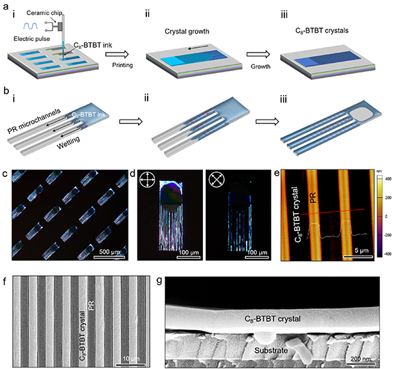
Figure 1. (a) Schematic illustration of the MA-IJP process for the patterned C8-BTBT crystals. (b) COMSOL simulations of the solution wetting process. (c) CPOM image of the C8-BTBT crystal array. (d) CPOM images of the C8-BTBT crystals at the same region under 45° and 0° polarization angles, respectively. (e) AFM image of the C8-BTBT crystals within the microchannel. (f) SEM image of the C8-BTBT crystals. (g) Cross-section SEM image of the C8-BTBT crystal.
Download figure:
Standard image High-resolution imageFigure 1(c) shows the CPOM images of the patterned C8-BTBT crystal array fabricated from the MA-IJP method. We observed that most of the C8-BTBT crystals in the microchannels shined bright light under the CPOM, indicating that a majority of C8-BTBT crystals have good crystalline quality. Moreover, the C8-BTBT crystals uniformly filled the PR microchannels. When the long axis of the C8-BTBT crystals was rotated 45° to the axis of the crossed polarizers, the C8-BTBT crystal arrays emitted bright blue color light (figure 1(d), left). As the long axis of the C8-BTBT crystal is parallel to the polarizer, the C8-BTBT crystal arrays emitted slightly weaker light (figure 1(d), right). This change in intensity indicates that the C8-BTBT crystals are aligned in the microchannels. Nevertheless, in the square region, a ring-like aggregation of C8-BTBT crystals was formed at the edge of the square (figure S2, supplementary materials) because of the well-known 'coffee-ring' effect for the droplet during drying [24, 25]. The comparison result confirmed that the microchannels could effectively promote the uniform growth of organic crystals. AFM and SEM were carried out to study the surface morphology of the C8-BTBT crystals. It shows that the C8-BTBT crystals have a smooth surface with a low root mean square roughness (Rq ) of 1.38 nm (figure 1(e)). And the C8-BTBT crystals filled the whole microchannel regions, and there were no obvious defects in the crystals (figure 1(f)). Cross-section SEM image in the figure 1(g) shows that the thickness of the obtained C8-BTBT crystals is approximately 200 nm. In addition, the cross section of the crystals is smooth and well defined, indicating good crystallinity.
Next, 2D-GIXRD with a synchrotron x-ray source was used to examine the crystallinity of the patterned C8-BTBT crystal arrays. The size of the x-ray beam in the 2D-GIXRD is approximately 400 µm × 600 µm, which means that the entire structure of the C8-BTBT crystals in each pattern area can be detected. Figure 2(a) shows a schematic illustration of the 2D-GIXRD measurement. The placement of the sample is ∼260 mm away from the 2D charge coupled device detector. The incident angle of an x-ray beam was set as 0.2° from the position of the reflected x-ray beam to the substrate. There are three Bragg diffraction spots at qz = 2.1, 4.3, and 6.5 nm−1 produced by C8-BTBT crystals in the 2D-GIXRD pattern (figure 2(b)), which can be assigned as the (001), (002), and (003) planes, respectively. The (00l) diffraction spots along the out-of-plane direction demonstrate the orientation of the C8-BTBT molecules and high-quality crystallinity. In addition, the patterned C8-BTBT crystal arrays appeared a series of intense spot-like diffractions along the in-plane direction (qxy ), which can be indexed to (11l).
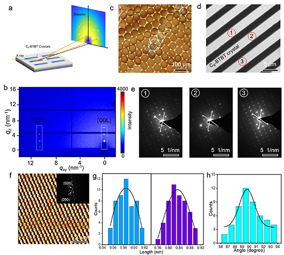
Figure 2. (a) Experimental setup for the 2D-GIXRD measurement. (b) 2D-GIXRD pattern of the patterned C8-BTBT crystals. (c) Optical microscopy and (d) corresponding TEM image of the C8-BTBT crystals on the Cu grid. (e) SAED patterns of the 1D C8-BTBT crystal collected from the marked areas (1–3) in (c). (f) HR-AFM image of the 1D C8-BTBT crystal. Inset: the corresponding Fourier transfer pattern. (g), (h) Histogram of lattice constants of the resulting C8-BTBT crystal array.
Download figure:
Standard image High-resolution imageFurthermore, TEM and selected-area electron diffraction (SAED) are used to assess the crystallographic orientation of the C8-BTBT crystals. We first transferred the sample from SiO2/Si to a Cu grid for TEM measurement according to our previous report (more details of the transfer method are shown in the figure S3) [26]. Figure 2(c) shows the optical microscopy image of the patterned C8-BTBT crystal array on the Cu grid. The pattered structure of C8-BTBT crystals was completely preserved. The corresponding TEM image further revealed the smooth surface of the crystals (figure 2(d)). SAED patterns obtained from three different C8-BTBT crystals in one pattern region present sharp diffraction spots and similar diffraction patterns (figure 2(e)), indicating that the crystals have a high crystalline quality and almost identical crystal orientation. Further, according to the TEM image and the corresponding SAED patterns, we can determine that the zone axes [010] are parallel to the growth direction of the C8-BTBT crystal. Moreover, a high-resolution AFM (HR-AFM) test is used to reveal the C8-BTBT molecular packing mode within the crystals. Fifty positions with an area of 10 × 10 nm2 are randomly collected from the same sample and all of the results exhibit a very similar molecular packing mode (figures 2(f) and S4, supplementary materials). The corresponding fast Fourier transform patterns of the HR-AFM images collectively demonstrate that the C8-BTBT crystals have an orthorhombic crystal structure with lattice constants of a = 5.9 ± 0.3 Å, b = 8.3 ± 0.8 Å, and γ = 91.2° ± 3.6° (figures 2(g) and (h)). These values are consistent with those of the C8-BTBT bulk crystals [27, 28].
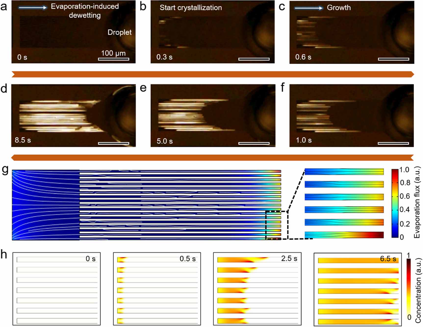
The unidirectional dewetting process occurring in the microchannels plays an important role in suppressing the disordered crystallization. We conducted in-situ observations to reveal the whole crystal formation process. Figures 3(a)–(f) exhibits the snapshots of the in-situ CPOM images, which are extracted from movie S1. At the first stage, only the organic ink existed in the microchannels and thus the CPOM image was dark (figure 3(a)). As the solvent evaporated, the C8-BTBT nucleation and crystallization preferentially occurred at the front of microchannels (figure 3(b)). With solvent continued evaporation, the solution dewetting was triggered and the crystals would grow along the dewetting direction simultaneously (figures 3(c)–(f)). To gain further insights into the underlying crystallization mechanism during the dewetting process, we performed computational fluid dynamics (CFDs) simulations. Figure 3(g) shows the evaporation flux (J) of the solution and solute concentration distribution (c) in the PR microchannels. The front-end solution J is thousands of times higher than the remaining parts, because the specific surface area of the front-end solution was much larger than that of the remaining parts. Thus, the solvent would continuously replenish and form convective flow that could transport molecules into this position, leading to the C8-BTBT supersaturated phase at the microchannel front. This would ensure preferential nucleation at this position. Figure 3(h) and movie S2, supplementary material exhibit the C8-BTBT concentration distribution within the microchannels during the solvent evaporation. In the whole dewetting process, the largest C8-BTBT concentration points were always located at the front end of the microchannels and retreated along the dewetting direction. This behavior could intensively suppress the random growth of the C8-BTBT crystals, allowing long-range ordered crystallization.
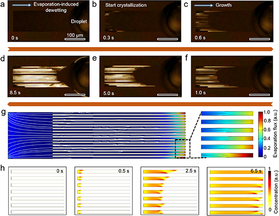
Figure 3. (a)–(f) In situ CPOM observation of the growth of C8-BTBT crystal in the microchannels. (g) Simulation evaporation of the C8-BTBT ink within the microchannels. (h) Simulation results of the dewetting process.
Download figure:
Standard image High-resolution imageThe width of the PR microchannels has a certain effect on the morphology of the resulting crystals. To clarify this, microchannels with different widths of 3, 4, 5, and 6 µm at an identical channel depth of ∼1 µm were used for comparison. Figure S5(a), supplementary materialpresents CPOM images of the C8-BTBT crystals obtained under different widths of microchannels. As the channel width increased, the crystal could only fill the front end of the microchannels due to the insufficient amounts of C8-BTBT molecules in the square regions. With the increasing of the amount of the ink, the obtained crystals would fill into the entire microchannels (figure S5(b), supplementary materials). The primary concentration of C8-BTBT ink also plays an important role in deciding the crystal morphology within the microchannels (figure S6, supplementary materials). When the ink concentration is low, the crystal only filled the front of the channels, and with the increase of the concentration, the length of crystals in the microchannels gradually increased. It is noteworthy that when the concentration reaches 10 mg ml−1, the C8-BTBT crystals appeared serious accumulation in the microchannels. In addition, our MA-IJP method also shows universal compatibility, patterned crystal arrays based on other soluble organic small molecule semiconductor, such as TIPS-pentacene, can be fabricated (figure S7, supplementary materials). The universality of the MA-IJP method is superior to our previous method [9], which only be applicable to liquid crystalline organic semiconductors.
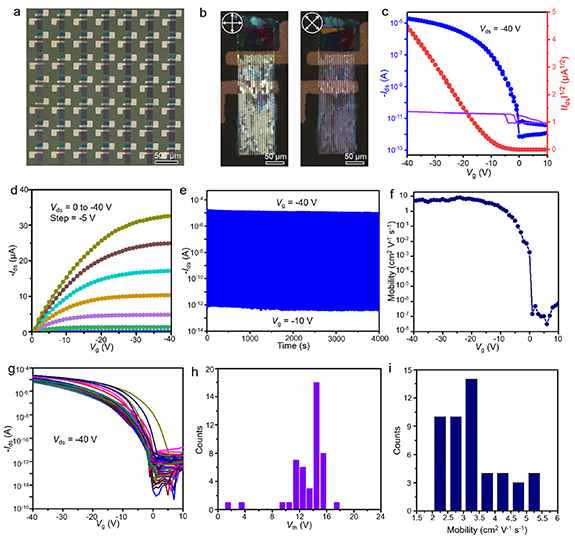
The MA-IJP method is able to deposit a patterned C8-BTBT crystal array with ordered orientation, which enables us to construct discrete OFETs with a low crosstalk effect. Figure 4(a) presents an optical microscope image of the 7 × 7 OFETs array made from the patterns of C8-BTBT crystals. The construction of the OFETs was a bottom-gate top-contact configuration, and the devices were fabricated on the BCB-coved SiO2/Si substrate. The capacitance of the double-layer dielectric layer was measured to be 7.35 nF cm−2 (figure S8, supplementary materials). The electrodes of the S and D were Ag, and a 2 nm thick F4-TCNQ layer was inserted into the interface between the C8-BTBT crystals and S/D electrodes, which could reduce the contact resistance [29, 30]. The effective channel L and W are 50 and 50 µm, respectively. All the 1D C8-BTBT crystals completely covered the channel of the OFET (figure 4(b)). Figures 4(c) and (d) show the transfer and output curves of one representative OFET in the 7 × 7 device array. The OFET displays an ideal p-type characteristic and has a good linearity, negligible hysteresis, and a very low leakage current. The mobility of the OFET reaches as high as 5.36 cm2 V−1 s−1, and the Ion/Ioff current ratio was estimated to be >107, along with the threshold voltage (Vth) of about −7 V. This mobility value is comparable to the previous reports for C8-BTBT crystals [31–34]. We also tested the transition curve of the linear region, and mobility in liner region was 5.01 cm2 V−1 s−1 (figure S9(a), supplementary materials). The excellent electrical characteristics could be attributed to the high crystalline quality of the C8-BTBT crystals. In addition, the OFET has a quite small bias stress effect (figure S9(b), supplementary materials), along with outstanding operating stability in the dark with a switching cycle of >4000 times (figure 4(e)). Figure 4(f) shows the saturation mobilities extracted under different gate voltages (Vg), and the mobility is almost gate-independent as Vg is above −10 V.
Figure 4. (a) CPOM image of the patterned C8-BTBT crystal-based 7 × 7 OFET array. (b) CPOM images of a representative OFET device. (c) Typical transfer and (d) output curves obtained from an OFET in the 7 × 7 device array. The purple-colored line represents the leakage current of the device. (e) Operational cycle stability of a representative OFET in air. (f) Extracted mobility as a function of Vg. (g) Transfer characteristics of the 49 OFETs recorded from the 7 × 7 device array. Statistical distribution of (h) Vth values and (i) mobilities.
Download figure:
Standard image High-resolution image
In order to evaluate the performance uniformity of the OFETs array, the whole OFETs in the 7 × 7 device array were measured. Figure 4(g) presents all the transfer curves of the 49 OFETs measured at the saturation regions. All the 49 OFETs can work properly with the similar transfer curves, suggesting that the patterned C8-BTBT crystals can effectively eliminate the crosstalk effect. Figures 4(h) and (i) show the histogram of the Vth and mobilities measured from the 7 × 7 OFET array, and the statistical values of Vth and mobility conformed to the normal distribution. It is worth noting that the Vth and mobility exhibit an obvious fluctuation. This is possibly attributed to the uneven quality and orientation of crystals in the different microchannel pattern region. The maximum and average mobilities of 49 OFETs are 5.36 and 3.23 cm2 V−1 s−1, respectively. The mobilites are lower than in our previous report [9], and it is expect to improve the mobilities through optimizing the thicknesses of the C8-BTBT crystals and improving the crystallinity. But these two values are remarkably higher than those of amorphous silicon, which can meet the specifications of the practical applications. At the same time, a patterned TIPS-pentacene crystals array was also fabricated for bottom gate top contact OFET devices, and the mobility of the TIPS-pentacene based OFET reached 1.83 cm2 V−1 s−1. This result proved that the MA-IJP method has good universality in constructing high-performance OFETs.
4. Conclusion
In summary, we have developed a facile and versatile MA-IJP method that enables the low-cost fabrication of a patterned OSCC array with well-oriented orientation. In this approach, microscale PR channels were introduced to manipulate the wetting and dewetting dynamics of organic inks, which could guide the unidirectional dewetting and ordered packing of molecules. The roles of the microchannels in controlling wetting and dewetting processes were verified through in situ microscopy observations and quantitative CFD simulations. The resulting patterned C8-BTBT crystal arrays showed high crystal quality and pure crystallographic orientation. Based on the patterned C8-BTBT crystals, a high-performance OFETs array with a yield of 100% was demonstrated. The maximum and average mobilities of the 7 × 7 OFET array are 5.36 and 3.23 cm2 V−1 s−1, surpassing those of the commonly used amorphous silicon transistors. The superiority of this approach to fabricate well-oriented OSCC arrays allows us to achieve high-performance organic integrated devices.
Acknowledgments
This work was supported by the National Natural Science Foundation of China (Grant Nos. 51973147, 61904117, and 52173178), Suzhou Key Laboratory of Functional Nano & Soft Materials, and Collaborative Innovation Center of Suzhou Nano Science and Technology (Nano-CIC). The authors thank the beamlines BL16B1 (Shanghai Synchrotron Radiation Facility) for providing the beamtime.
Data availability statement
The data that support the findings of this study are available upon reasonable request from the authors.