
Abstract
A tandem device which integrates a PVDF nanogenerator and silicon (Si) nanopillar solar cell is fabricated. The Si nanopillar solar cell was fabricated using a mask-free plasma etching technique and annealing process. The PVDF nanogenerator was stacked on top of the Si nanopillar solar cell using a spinning method. The optical properties and the device performance of nanowire solar cells have been characterized, and the dependence of device performance versus annealing time or method has been investigated. Furthermore, the PVDF nanogenerator was operated with a 100 dB sound wave and a 0.8 V peak to peak output voltage was generated. This tandem device can successfully harvest energy from both sound vibration and solar light, demonstrating its strong potential as a future ubiquitous energy harvester.
Export citation and abstract BibTeX RIS
Recently attention has been paid to the harvesting of ubiquitous energy such as solar energy, mechanical energy, and thermal energy as energy sources for low-power electronics. Photovoltaic (PV) cells based on nanostructures such as Si nanorods (SiNR) [1], Si nanocones (SiNC) [2], Si nanowires (SiNW) [3, 4], and Si nanopillars (SiNP) [5, 6] have been proposed as a promising candidate for solar energy harvesting due to their excellent optical [7–9] and electrical [10–12] performance. These nanostructure solar cells have certain advantages, such as (i) low reflection due to the density-graded surface [12], (ii) high absorption due to the strong diffraction and scattering on the nanostructure surface [13, 14], and (iii) compatibility with low-grade Si raw materials for low-cost mass production [2, 15].
On the other hand, considerable efforts have been made to harvest mechanical energy, such as sound vibration, air or water flow and vibration from human motion. Various piezoelectric nanogenerators, such as ZnO nanowires [16–19], PVDF polymers [20], and BaTiO nanoparticles [21] have been studied for conversion of mechanical energy into electrical energy. However, these solar cells and nanogenerators require specific environmental conditions, such as solar light and mechanical vibration. Thus, there is an increasing demand for a hybrid system that utilizes two or more energy sources in order to harvest ubiquitous energy continuously.
In this study, a tandem device integrating a Si nanopillar (SiNP) solar cell and a PVDF nanogenerator was fabricated using a mask-free plasma etching process and a spin coating method. Its optical and electrical properties were investigated for solar cell application and vibration energy harvesting. The output power was generated from both light illumination and sound generation. This tandem device showed 3.29% solar conversion efficiency and a 0.8 V peak to peak AC output voltage via 100 dB sound generation. With this hybrid device, both solar and vibration energies were converted to electrical energy. This result demonstrated that more efficient energy harvesting from the ambient environment is possible using this hybrid device.
A p-type multi-crystalline Si (mc-Si) wafer with a resistivity of 0.5–3 Ω cm was loaded onto the chuck of an inductively coupled plasma (ICP) etcher with a thermal paste for cooling the sample temperature during the etching process. The chamber pressure and ICP/bias power were set constant at 30 mTorr and 600/30 W, respectively. The O2/SF6 ratio and etching time for nanostructure formation were optimized experimentally, and were 1.80 and 150 s, respectively, for the SiNP arrays [22]. Subsequently, the samples were cleaned in piranha solution (H2O2:H2SO4 = 1:1) at 100 °C for 20 min and buffered HF (aqueous, HF:NH4F = 1:6) at room temperature for 10 s in order to remove the organic residue and the surface oxide layer, respectively. An n+–p vertical-junction was formed by a spin-on-dopant process. The n-type dopant material was phosphorus (Filmtronics, P509). The dopant spin coating speed was 2500 rpm for 30 s. The dopants were activated by furnace annealing at 900 °C for 7 min or rapid thermal annealing (RTA) at 900 °C for 30 s. The samples were then coated with an indium tin oxide (ITO) film via RF sputtering. The thickness of deposited ITO ranged from about 20 to 40 nm. For the solar cell measurement, silver (Ag) and aluminum (Al) were deposited as front and back electrodes, respectively, via thermal evaporation. An annealing process in a N2 environment at 400 °C for 4 min was applied to form ohmic contact at the Al–Si interface and to enhance the transparency of ITO. The schematic of the SiNP solar cell is shown in figure 1(a). After fabricating the Si nanopillar solar cells, the PVDF nanogenerator was then fabricated. Nafion (0.5 wt% in ethanol) was coated onto the top of the Si nanopillar solar cell template as a self-assembled monolayer (SAM) treatment to promote the wetting properties of the PVDF solution. The PVDF solution was then spin-coated in methyl ethyl ketone (MEK). Thermal annealing was carried out at 80 °C for 2 h. After the formation of the PVDF piezo-polymer layer, an ITO coated polyethersulfone (PES) substrate was attached onto the top of the layer as both a top electrode and a vibration plate. The electrodes were connected to both the ITO coated PES substrate and the ITO coated SiNP surface. Figure 1(b) shows a schematic of the hybrid system of the PVDF nanogenerator and NP–Si solar cell. Pillar structures of polycrystalline silicon were fabricated using an inductively coupled plasma (ICP) etcher [22]. At the beginning of the plasma etching process, a passivation layer is formed on the silicon surface, mainly from the reaction of silicon with oxygen radicals generated from the O2/SF6 plasma. The development of the formed SiOxFy passivation layer which is generated during the plasma etching process determines the nanostructures as shown in figure 2(a). The model of the nanostructure's temporal evolution is proposed in figure 2(b). The mechanism of pillar growth can be explained as follows. Uneven nanostructures on the surface are developed in the early stage of the etching process by the non-uniform formation of the passivation layer across the surface. The sidewall of the nanostructures is also etched as the etching progresses, resulting in the elimination of relatively thin pillars and the increased lateral spacing between nanopillars. Figures 2(c) and (d) show the top and side view, respectively, of field effect scanning electron microscope (FESEM) images of typical self-assembled pillar structures that can be fabricated by using plasma etching. The typical height and diameter of the pillars are 0.9 μm and 300 nm, respectively. ITO coating on the nanostructures follows after the formation of nanostructures. The ITO layer, which acts as transparent conducting oxide (TCO), collects separated charges from the nanostructure and transports them to the front electrode.

Figure 1. (a) Schematic diagram of the SiNP solar cell. (b) Schematic diagram of the hybrid energy harvester: a PVDF NG was integrated on top of the SiNP solar cell.
Download figure:
Standard image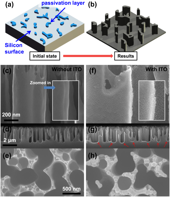
Figure 2. (a) Schematic model for the self-assembled random passivation layer. (b) Schematic model for the fabrication process of the self-assembled random Si nanostructure. (c)–(e) SEM images of Si NW solar cells before ITO deposition. Small (c) and large (d) area cross-sectional and top (e) views. (f)–(h) SEM images of Si NW solar cells after ITO deposition. Small (f) and large (g) area cross-sectional and top (h) views. (c) and (f) show the clear ITO deposition at the sidewall of the nanopillars. (d) and (g) show the clear ITO deposition at the bottom of the nanopillars. The red arrows indicate the deposited ITO at the bottom. (e) and (h) show the clear ITO deposition at the top of the nanopillars.
Download figure:
Standard imageThe coverage of ITO deposition is confirmed by SEM images from both the top and side views, as shown in figure 2. The top view images (see figure 2(e)) suggest that the ITO film provided a reasonable coverage of the active device area for SiNP samples, compared to those before ITO deposition (see figure 2(c)). The side view images of SiNP before and after ITO deposition are shown in figures 2(d) and (f). The ITO films on the top, side and bottom of the SiNP arrays have a relatively uniform thickness of between ∼20 and ∼40 nm. As shown in figure 2, the SEM pictures verify the uniform coverage of the ITO on the nanopillar structure. By comparing SEM images of the nanopillars with and without ITO deposition, we confirmed that the side and bottom of the nanopillars are well covered by the ITO.
Figure 3(a) shows the reflectance measured from the pillar nanostructures with and without ITO coating. The result shows that there is no significant difference between that reflectance from the pillar structured surface and that from the surface with subsequent ITO deposition. This indicates that the ITO coating on the pillar nanostructure is almost transparent in the wavelength range from 200 to 1400 nm. The current density–voltage (J–V) characteristics with and without light illumination for the SiNP arrays are shown in figure 3(b), which shows the electrical properties. In figures 3(c) and (d), Voc and Jsc versus annealing method/times are plotted. Since the n+ layer is formed during the annealing process, the annealing step is a crucial process in fabricating the p–n junction in the SiNP solar cells. There is no significant difference in Voc at ∼0.5 V despite the change of process condition. On the other hand, the short circuit current density decreases with increased furnace annealing time because the junction depth increases as the annealing time increases. This results in a decrease of the volume of the p-core region inside the nanostructures, which results in a decrease in the total area of the p and n interface. Therefore, the total photo-generated current decreases. The cell efficiency and fill factor are plotted in figures 3(e) and (f). The conversion efficiency and the fill factor decrease as the annealing time increases because the short circuit current density decreases with increasing annealing time.

Figure 3. (a) Reflectance versus wavelength of NP–Si with and without ITO coating. (b) J–V characteristics of the NP silicon solar cell with and without illumination. (c) Voc, (d) Jsc, (e) efficiency, and (f) fill factor with respect to annealing methods and times. The red dot on the left indicates the RTA process and the black lines indicate the furnace process for different annealing times.
Download figure:
Standard imageThe efficiency and fill factor of the pillar structured device of which the junction is formed by RTA are higher than those formed by furnace annealing (figures 3(e) and (f)). This is because RTA can produce a thinner n+ junction which can enhance the diode characteristics because of higher activation and suppressed diffusion of the n-type phosphorus dopants [23]. According to the diffusion equation, the thickness of the doping layer increases with increasing annealing time. Therefore, if the annealing time becomes shorter, the thickness of the doping layer becomes thinner, even at the same temperature [24].
Figure 4(a) shows a side view of the PVDF polymer coated on top of the Si nanowires. PVDF polymer is coated conformally on the ITO coated Si nanopillar surface due to the MEK SAM treatment. With the 4 wt% PVDF solution, the thickness of the PVDF film is 1.5 μm when the SiNW length is 1 μm. The transmission of 1.5 μm thick PVDF thin film is about 88%–93% in the visible range. In order to operate the hybrid system, we tested the Si solar cells and PVDF piezogenerator separately. The PVDF piezoelectric nanogenerator was operated by sound waves with a 100 dB power and 100 Hz frequency and a 0.8 V peak to peak output potential was generated from the PVDF piezoelectric generator, as shown in figure 4(b). For the SiNW PV device, red light (with the wavelength centered at 630 nm) was illuminated on top of the hybrid devices and switched on and off using an optical chopper. A 430 mV photovoltaic potential was recorded on the oscilloscope, as shown in figure 4(c). Finally, the generated output voltage from the Si–PV cells and PVDF nanogenerator were added while vibrating the top PES substrate with sound waves and modulating the light illumination with the optical chopper. As shown in figure 4(d), the clear on and off output voltage from the PV cell, and the 100 Hz frequency AC modulation from the sonic wave, were generated.
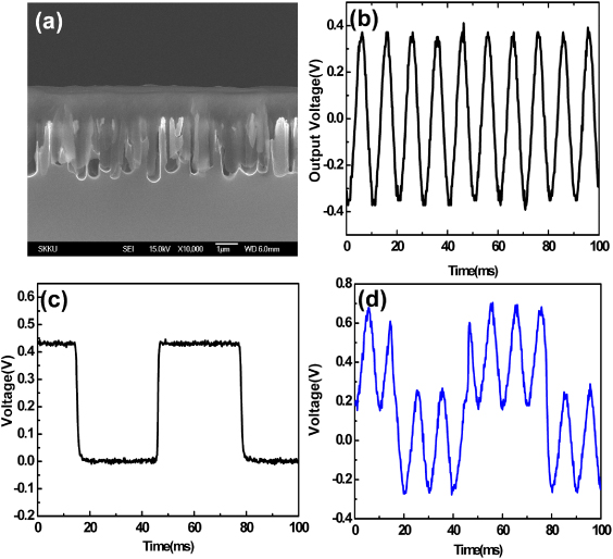
Figure 4. (a) Side view of the FESEM image of the hybrid energy harvester: PVDF coated on top of NP–Si. (b) Output voltage generated by the 100 dB sound wave with a 100 Hz frequency. (c) Photovoltaic potential generated by modulated light illumination with chopper. (d) Potential generated by both light modulation and 100 dB sound wave.
Download figure:
Standard imageIn conclusion, a tandem hybrid device using a SiNP solar cell and a PVDF NG was fabricated. The SiNP solar cell was fabricated using a plasma etching technique and doping process by rapid thermal annealing (RTA) and furnace annealing. The PVDF NG was stacked on top of the SiNP solar cell using a spin coating method. The performance and mechanism of photovoltaic effects from the SiNP solar cells was investigated. The device was simultaneously operated using light illumination and sound vibration. With this tandem hybrid device, a photo-generated voltage and a vibration generated AC voltage are successfully generated, demonstrating that the SiNP solar cells and PVDF tandem device is a promising method for harvesting both photo and vibration energy.
Acknowledgments
This research was supported by the Basic Science Research Program through the National Research Foundation of Korea (NRF) funded by the Ministry of Education, Science and Technology (2009-0083540, 2011-0010274). DJK and ARJ also wish to acknowledge the financial support by WCU (World Class University) program (R31-2008-000-10029-0), Center for Advanced Soft Electronics under the Global Research program (2011-0032153) through the National Research Foundation of Korea (NRF) funded by the Ministry of Education, Science and Technology.